Standard PCB Layout Guidelines
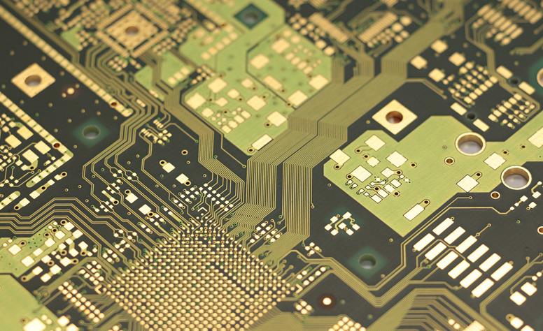
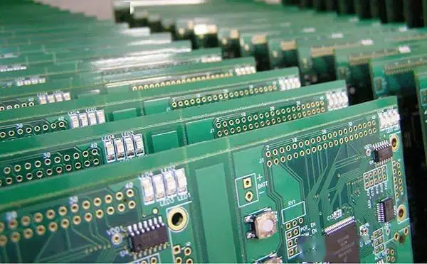
PCB (Printed Circuit Board) layout design directly impacts the performance, stability, and manufacturing cost of a product. Following proper layout principles can enhance signal integrity, reduce electromagnetic interference (EMI), and improve production efficiency. Below are the key guidelines for PCB design:
1. Component Layout Principles
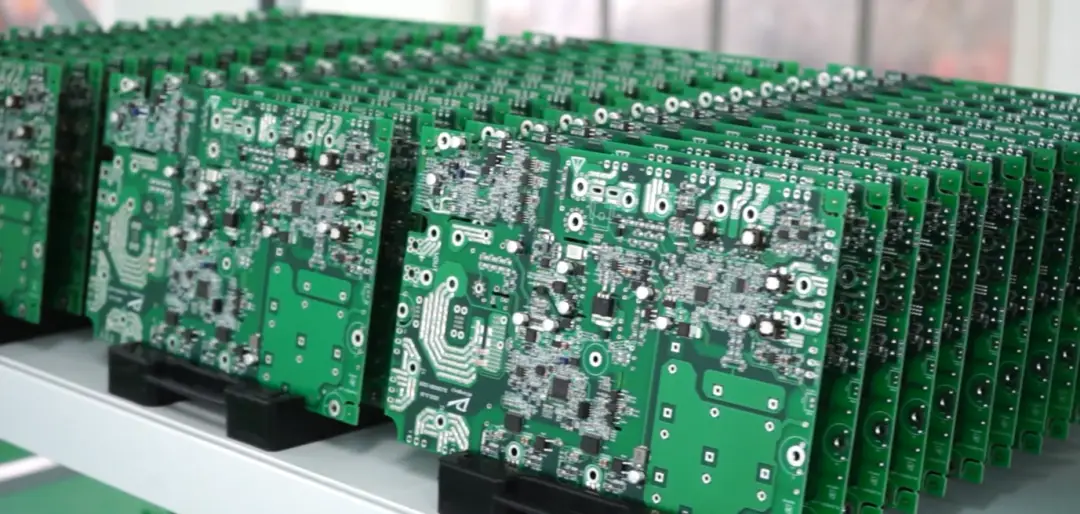
Functional Partitioning: Place components by functional areas, such as power, circuit control, and signal processing, to reduce interference and improve maintainability.
Thermal Management: High-power components should be placed away from temperature-sensitive components, and heat dissipation copper or vias should be arranged to ensure even temperature distribution.
Mechanical Constraints: Pay attention to the distance between components and the board edges or mounting holes to avoid processing and assembly issues.
2. Routing Rules
Signal Integrity: Keep high-speed signals as short and direct as possible, avoiding 90° bends to reduce reflection and crosstalk.
Power and Ground Lines: Use a solid ground plane to ensure low-impedance return paths. Increase the width of power lines to reduce voltage drop.
Differential Signals: Maintain equal length and spacing to ensure impedance matching and minimize interference.
3. Electromagnetic Compatibility (EMC) Design
Minimize Loop Area: Keep signal loops short to prevent large current loops that can cause EMI.
Shielding Design: Add grounding shields or metal enclosures to critical circuits to improve resistance to interference.
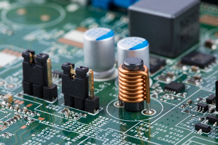
Filtering and Decoupling: Add filtering capacitors at power entry points and matching resistors to critical signals to reduce high-frequency noise.
4. Manufacturability and Testability
Appropriate Trace Spacing: Follow manufacturing process standards to ensure trace width, spacing, and pad sizes are compatible with fabrication capabilities, avoiding short circuits or open circuits.
Test Points: Include test points at critical locations for easy circuit diagnostics and improving production yield.
Via Optimization: Minimize unnecessary vias to avoid increasing manufacturing costs and signal loss.
Newway Industrial – Professional PCB Solution Provider
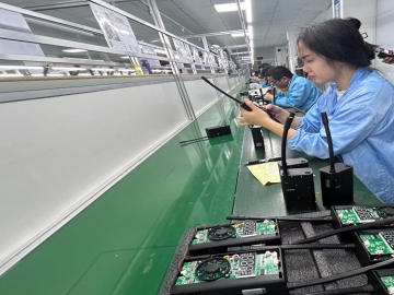
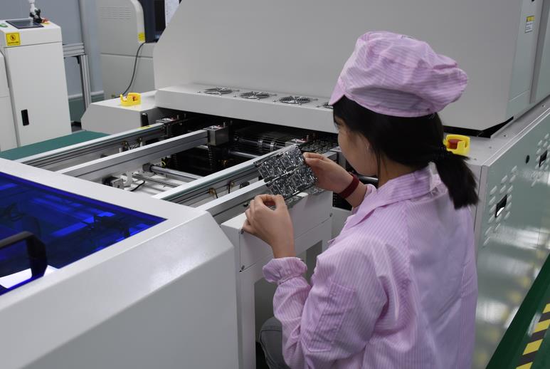
Newway Industrial has been a trusted name in the PCB industry for years, providing high-quality PCB design, manufacturing, and customized services. The company boasts advanced PCBA production lines and a rigorous quality management system, having obtained certifications such as ISO9001 and BSCI, ensuring products meet international standards like 3C, CE, FCC, and RoHS. Newway Industrial offers one-stop OEM/ODM solutions and specializes in high-precision, high-reliability PCB manufacturing, widely used in communication devices, medical electronics, industrial control, automotive electronics, and more. Choosing Newway Industrial means choosing professionalism and quality assurance.
<!--!doctype-->
Tags: PCBA /PCB Layout /
Prev: Neway Industry Showcases One-Stop PCBA Solutions at 2025 ITES Shenzhen Industrial Exhibition
Next: No more...


