What does PCB embedded component design mean?
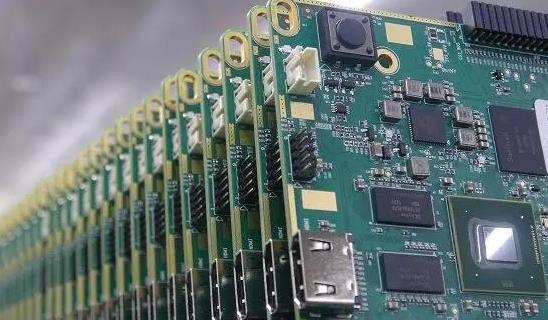
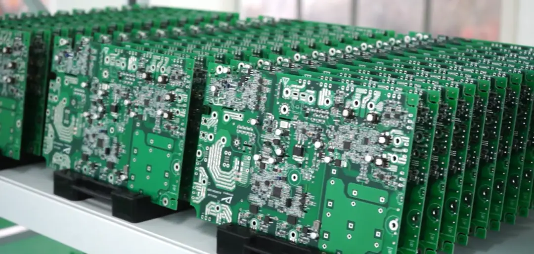
PCB buried component design refers to a circuit board design technique where electronic components are embedded into the internal layers of the circuit board, rather than being placed traditionally on the top or bottom surfaces. This design approach is primarily aimed at meeting the demand for smaller and more integrated electronic products, as well as improving circuit signal frequency and performance.
Specifically, PCB buried component design has the following key points:
Increased integration: By embedding components into the internal layers of the circuit board, it significantly enhances the integration level, reduces the circuit board size, and thus meets the miniaturization requirements of modern electronic products.
Improved signal performance: As the components are embedded inside the circuit board, it shortens the signal length, reduces resistance and parasitic inductance, thereby lowering noise and EMI (electromagnetic interference), and improving circuit signal integrity.
Enhanced reliability: Since the components are embedded inside the circuit board, they are protected from external environments such as dust and humidity, improving the reliability of the circuit.
Design flexibility: In PCB design tools, components can be placed on any signal layer, not just the traditional top or bottom surface signal layers, providing greater flexibility for designers.
PCB buried component design primarily includes two types of embedded components:
Embedded discrete components: Such as surface mount resistors and capacitors, which are placed on the inner layers of the circuit board during manufacturing/assembly.
Embedded integrated components: These components are formed directly on the inner layers during the manufacturing process of the circuit board, such as 3M-CPly.
PCB buried component design is an advanced circuit board design technique that provides strong support for the development of modern electronic products by increasing integration, improving signal performance, enhancing reliability, and providing design flexibility.
Prev: What does EMS mean in Printed Circuit Board Manufacturing?
Next: Why is multilayer ceramic PCB harder to build?


