How is a PCB manufactured step-by-step?
The manufacturing of a PCB (Printed Circuit Board) involves several precise and intricate steps. Here's a simplified, step-by-step overview of the process:
Design and Engineering:
The process begins with the creation of the PCB design using design tools like Altium, Eagle, KiCad, etc..
Engineers determine the board's size, shape, component placement, and routing of electrical traces, ensuring adherence to industry standards and specifications.
Artwork Generation:
Once the design is approved, it is converted into digital artwork files, typically in Gerber format.
These files contain detailed information about the board's layout, including copper traces, solder mask, and other features, which guide the subsequent fabrication processes.
Preparation of Base Material:
The base material (usually copper-clad laminate) is prepared for processing.
This involves cleaning and preparing the surface for the next steps.
Photoresist Application:
A photoresist, a light-sensitive material, is applied to the bare copper surface of the PCB.
This layer will be exposed to UV light in subsequent steps, selectively hardening it in the areas where copper traces are desired.
UV Exposure and Development:
The photoresist-coated PCB is exposed to UV light through a mask containing the desired circuit pattern.
The UV light hardens the exposed areas of the photoresist, while the unexposed areas remain soft.
The PCB is then subjected to a development process, where the unexposed photoresist is dissolved, leaving behind a protective layer over the desired copper traces.
Etching:
The PCB is submerged in an etching solution, which selectively dissolves the exposed copper (not protected by the photoresist).
This removes the unwanted copper, leaving behind the desired circuit pattern.
Stripping and Cleaning:
After etching, the residual photoresist is removed from the PCB through a stripping process.
The board is thoroughly cleaned to remove any remaining contaminants or debris.
Solder Mask Application:
A solder mask, a protective layer, is applied to the PCB to prevent solder bridges and shorts between adjacent copper traces.
This layer is typically applied through a screen printing process and can be customized with colors and markings for identification purposes .
Silkscreen Printing (Optional):
In some cases, a silkscreen layer containing component identifiers, reference designators, and other information is applied to the PCB.
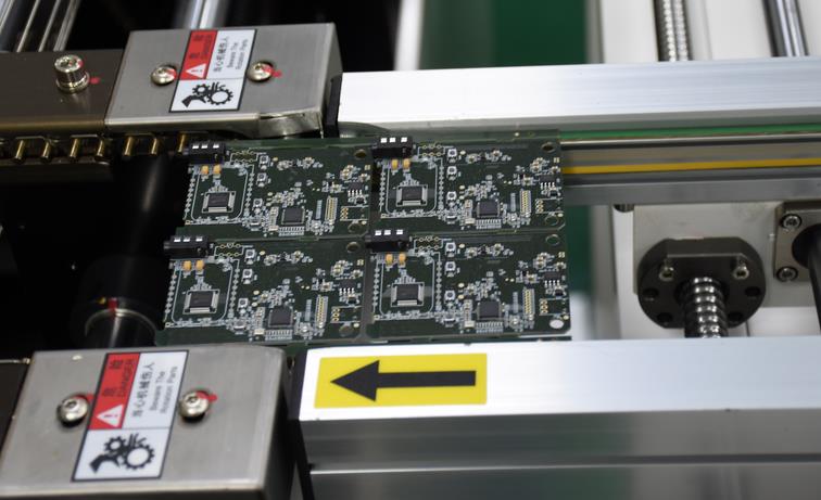
Assembly:
Components are placed and soldered onto the PCB, either manually or through automated processes like SMT (Surface Mount Technology) or THT (Through-Hole Technology).
Inspection and Testing:
The completed PCBAs undergo rigorous inspection and testing to ensure they meet quality standards and perform as designed.
This process can vary slightly depending on the specific type of PCB (e.g., single-sided, double-sided, or multilayer) and the manufacturer's equipment and processes.
Tags: PCB /PCB_manufactured /
Prev: What is the PCBA reliability test standard?
Next: How much does it cost to prototype a PCB?


