What are the steps of PCB assembly?
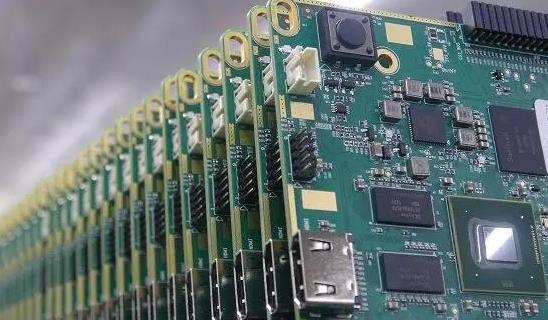
PCB assembly involves several steps to transform a bare printed circuit board into a functional electronic device. Here are the typical steps involved in PCB assembly:
Component Procurement: The first step is to procure all the electronic components required for the PCB assembly. These components can include resistors, capacitors, integrated circuits, connectors, and other specialized parts.
Stencil Creation: If surface-mount technology (SMT) components are being used, a stencil is created to apply solder paste to the bare PCB. The stencil ensures precise deposition of solder paste onto the pads where components will be mounted.
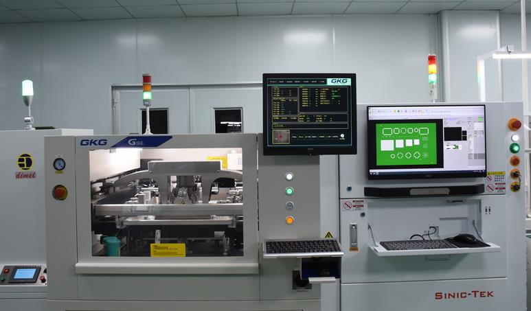
Solder Paste Printing: Using the solder paste stencil, solder paste is applied to the pads on the bare PCB using a stencil printer. This step ensures that the right amount of solder paste is deposited on each pad.
Component Placement: Automated pick-and-place machines or manual labor is used to accurately place the electronic components onto the solder paste on the PCB. This step requires careful alignment and positioning of components according to the PCB design.
Reflow Soldering: The assembled PCB is passed through a reflow oven where the solder paste is heated, melting the solder and forming the electrical connections between the components and the PCB pads. This process typically involves multiple heating zones to ensure proper soldering.
Through-Hole Component Insertion (if applicable): If through-hole components are used in addition to SMT components, they are inserted into the corresponding holes on the PCB manually or using automated insertion equipment.
Wave Soldering (if applicable): If through-hole components are present, the assembled PCB may undergo wave soldering. In this process, the bottom side of the PCB is passed over a wave of molten solder, which forms solder joints between the through-hole components and the PCB.
Inspection and Testing: After soldering, the assembled PCB undergoes visual inspection and testing to detect any defects such as soldering defects, component misalignment, or electrical issues. Automated optical inspection (AOI) and in-circuit testing (ICT) are commonly used for this purpose.
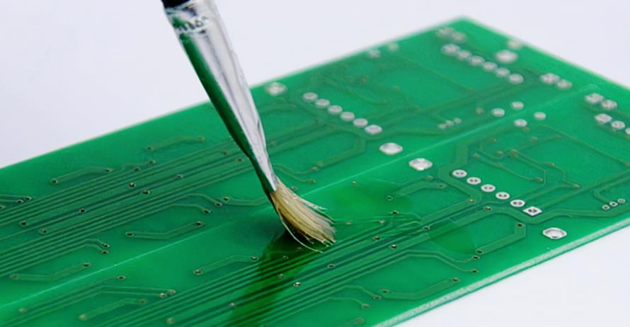
Cleaning (if applicable): If required, the PCB assembly may undergo a cleaning process to remove any residual flux or contaminants left from the soldering process. This ensures the long-term reliability of the PCB assembly.
Final Assembly and Packaging: Once the PCB assembly passes inspection and testing, any remaining assembly steps such as attaching connectors, mounting components, and final testing may be performed. The assembled PCBs are then packaged according to the specific requirements of the product.
These steps may vary slightly depending on factors such as the complexity of the PCB design, the type of components used, and the manufacturing processes employed by the assembly facility.
Tags: PCB_assembly /steps /
Prev: What does a PCB assembler do?
Next: Why use automated PCB assembly?


