
The basic requirements of SMT process for component layout design
The layout of components should be designed based on the characteristics and requirements of SMT electronic processing production equipment and processes. Different processes, such as reflow soldering and wave soldering, have different layouts for components. When double-sided reflow soldering, there are different requirements for the layout of side A and side B; Selective wave soldering and traditional wave soldering also have different requirements.
The basic requirements for component layout design in SMT process are as follows:
The distribution of components on printed circuit boards should be as uniform as possible. When reflow soldering high-quality components, the heat capacity is large, and excessive concentration can easily cause local low temperatures and lead to virtual soldering; At the same time, a uniform layout is also beneficial for center of gravity balance. In vibration and impact experiments, it is not easy to encounter damage to components, metalized holes, and solder pads.
The arrangement direction of components on printed circuit boards should be the same as much as possible for similar components, and the feature direction should be consistent to facilitate the installation, soldering, and testing of components. The positive electrode of electrolytic capacitors, the positive electrode of diodes, the single pin end of transistors, and the first pin of integrated circuits should be arranged in the same direction as much as possible. The printing orientation of all component numbers is the same.
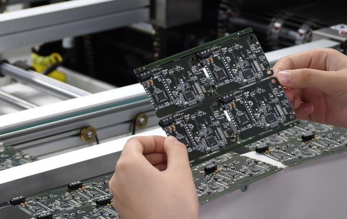
Large components should have a size around the SMD repair equipment heating head that can be operated.
Heating components should be kept as far away from other components as possible, generally placed in corners and ventilated positions inside the chassis. Heating components should be supported by other leads or other supports (such as heat sinks) to maintain a certain distance from the surface of the printed circuit board, with a minimum distance of 2mm. The heating element is connected to the printed circuit board in a multi-layer board, with a metal solder pad designed and soldered during processing to dissipate heat through the printed circuit board.
Temperature sensitive components should be kept away from heating components. For example, transistors, integrated circuits, electrolytic capacitors, and some plastic shell components, they should be kept as far away as possible from bridge stacks, high-power components, heat sinks, and high-power resistors.
The layout of components and parts that require adjustment or frequent replacement, such as potentiometers, adjustable inductance coils, variable capacitor microswitches, fuse tubes, buttons, plugins, etc., should consider the structural requirements of the entire machine and place them in positions that are easy to adjust and replace. If it is adjusted internally, it should be placed in a convenient place on the printed circuit board for adjustment; If it is adjusted outside the machine, its position should match the position of the adjustment knob on the chassis panel to prevent conflicts between three-dimensional and two-dimensional space. For example, the panel opening of the button switch should match the empty position of the switch on the printed circuit board.
Fixed holes should be set up near wiring terminals, plug-in components, the center of long string terminals, and frequently subjected to force, and corresponding space should be left around the fixed holes to prevent deformation due to thermal expansion. If the thermal expansion of long string terminals is more severe than that of printed circuit boards, it is easy to cause warping during wave soldering.
Some components and parts (such as transformers, electrolytic capacitors, varistors, bridge stacks, heat sinks, etc.) with large volume (surface) tolerance and low accuracy that require secondary processing, have an additional margin between them and other components based on the original setting.
It is recommended to increase the margin of electrolytic capacitors, varistors, bridge stacks, polyester capacitors, etc. by no less than 1mm, and transformers, heat sinks, and resistors exceeding 5W (including 5W) by no less than 3mm
Electrolytic capacitors should not touch heating components, such as high-power resistors, thermistors, transformers, heat sinks, etc. The minimum distance between electrolytic capacitors and heat sinks is 10mm, and the minimum distance between other components and heat sinks is 20mm.
Stress sensitive components should not be placed at the corners, edges, or near connectors, installation holes, slots, cuts, notches, and corners of printed circuit boards. These positions are high stress areas of printed circuit boards, which can easily cause cracking or cracking of solder joints and components.
The layout of components should meet the process requirements and spacing requirements of reflow soldering and wave soldering. Reduce the shadow effect generated during wave soldering.
Positions for positioning holes and fixing brackets on printed circuit boards should be reserved.
In the design of large-area printed circuit boards with an area exceeding 500cm2, to prevent bending of the printed circuit board during soldering, a gap of 5-10mm wide should be left in the middle of the printed circuit board, without placing components (which can be wired), to be used to add pressure strips to prevent bending of the printed circuit board during soldering.
The layout direction of components in reflow soldering process.
① The placement direction of components should consider the direction of the printed circuit board entering the reflow soldering furnace.
② In order to synchronize the heating of the solder joints on both sides of the two terminal chip components and the pins on both sides of the SMD components, and to reduce welding defects such as standing, shifting, and detachment of solder joints from the solder pads caused by the inability to synchronize heating on both sides of the components, it is required that the long axis of the two terminal chip components on the printed circuit board should be perpendicular to the direction of the conveyor belt of the reflow soldering furnace.
③ The long axis of SMD components should be parallel to the transfer direction of the reflow soldering furnace, and the long axis of Chip components at both ends should be perpendicular to the long axis of SMD components.
④ A good component layout design should not only consider the uniformity of thermal capacity, but also the direction and order of component layout,
⑤ For large-sized printed circuit boards, in order to maintain consistent temperature on both sides of the board, the long side of the printed circuit board should be parallel to the direction of the conveyor belt of the reflow soldering furnace. Therefore, when the size of the printed circuit board is greater than 200mm, the following requirements are required:
a) The long axis of the Chip component with two terminals is perpendicular to the long edge of the printed circuit board.
b) The long axis of SMD components is parallel to the long side of the printed circuit board.
c) A double-sided printed circuit board with identical orientation of components on both sides.
d) The arrangement direction of components on printed circuit boards should be the same as much as possible for similar components, and the feature direction should be consistent to facilitate the installation, soldering, and testing of components. The positive electrode of electrolytic capacitors, the positive electrode of diodes, the single pin end of transistors, and the first pin of integrated circuits should be arranged in the same direction as much as possible.
To prevent interlayer short circuits caused by touching printed wires during PCB processing, the conductive patterns on the inner and outer edges should be greater than 1.25mm from the edge of the PCB. When the outer edge of the PCB has already been laid with a grounding wire, the grounding wire can occupy the edge position. For PCB board positions that have already been occupied due to structural requirements, components and printed wires cannot be laid out again. There should be no through holes in the bottom solder pad area of SMD/SMC to avoid the solder being heated and remelted during peak soldering after reflow soldering and then diverted.
Installation spacing of components: The minimum installation spacing of components must meet the requirements of manufacturability, testability, and maintainability for SMT assembly.
Tags: SMT_process /component_layout_design /
Prev: How to control the quality of PCB boards in PCB factories?
Next: Notes on BGA layout design in PCBA processing


