Notes on BGA layout design in PCBA processing
1. Background Description
BGA has a large size and a small cross-sectional area of solder joints. When the PCB is bent, the solder joints at its four corners become stress concentrated areas. If the stress is too high in electronic processing, it may lead to solder joint cracking.
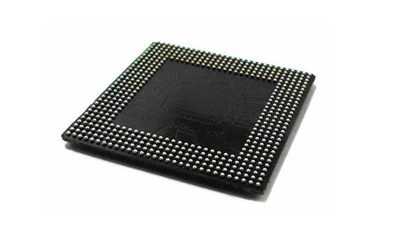
2. BGA Layout Design Requirements
(1) Try to layout the PCB as close to the transfer edge as possible, as the deformation during welding is relatively small.
(2) Try to avoid layout at the corners of L-shaped plates and near crimping connectors as much as possible.
(3) Try to avoid mirrored layouts on both sides as much as possible. If this layout is necessary, the PCB board thickness should be ≥ 2.0mm, mainly considering long-term reliability. This is based on research conclusions from multiple well-known enterprises, and the reliability of mirror layout BGA is reduced by more than 50%.
(4) PBGA should avoid layout on the first assembly surface (first welding surface, bottom surface) as much as possible.
(5) Try to avoid placing BGA near the separation edge of the assembly as much as possible.
Tags: PCBA_processing /BGA /BGA_layout /
Prev: The basic requirements of SMT process for component layout design
Next: Layout design requirements for chip capacitors in PCBA processing


