Layout design requirements for chip capacitors in PCBA processing
Layout design requirements for chip capacitors in PCBA processing
1. Background Description
Chip capacitors are a widely used type of packaging in various electronic processing products, among which multi-layer ceramic capacitors (MLCC) are the most commonly used. However, they have a serious drawback, which is the presence of stress effects. Stress cracking may occur when PCB bending reaches 2.4% or more. The direction of stress action is different, and the location of cracking is also different.
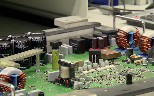
2. Layout design requirements for chip capacitors
(1) Chip capacitors should be kept as far away as possible from areas prone to deformation during assembly, such as around crimped connectors, screws, and inserts.
(2) When the layout of the chip capacitor is near the splicing connection bridge and stamp hole, the width of the cloth prohibition ring needs to be ≥ 12.5mm. It should be pointed out that the distance between the chip capacitor and the connection bridge and stamp hole depends on the layout board process method and board thickness. This value is a reference design requirement given under manual board splitting process conditions, and the specific requirements should also be determined according to the process of your own workshop.
(3) Chip capacitors should be kept as far away as possible from areas that are prone to stress during product application, such as around plug-in connectors, battery charging sockets, and buttons. If the layout is in these areas, the product design must ensure that the chip capacitors are not affected by stress during application.
(4) Chip capacitors should not be placed near the window wall of the selective wave soldering mask as they are prone to breakage due to thermal stress.
(5) Chip capacitors should not be placed around the nozzle selection welding points as much as possible, as they are prone to breakage due to thermal stress, especially when parallel to the radial direction.
Tags: PCBA_processing /capacitors /
Prev: Notes on BGA layout design in PCBA processing
Next: What are the reliability tests in the PCBA processing process?


