
Advantages of SMT surface assembly technology
As a new generation of assembly technology, SMT technology has only a history of more than 40 years, but this technology has fully demonstrated its strong vitality as soon as it was born. It has completed the journey from birth, perfection to maturity at an extraordinary speed and entered a prosperous period of large-scale industrial application. Nowadays, both investment electronic products and civilian electronic products have its presence. Why has SMT developed so fast? This is mainly due to the following advantages of SMT.
1. High assembly density
The area and mass occupied by chip components are greatly reduced compared with traditional perforated components. Generally, the use of SMT can reduce the volume of electronic products by 60% to 70% and the mass by 75%. Through-hole installation technology installs components according to a 2.54mm grid; while the grid of SMT assembly components has developed from 1.27mm to the current 0.5mm grid, and the density of installed components is higher. For example, a 64-pin DIP integrated block has an assembly area of 25mm×75m, while a QFP with the same lead spacing of 0.63mm has an assembly area of 12mm×12mm, which is 1/12 of the area of through-hole technology.
2. High reliability
Since chip components have high reliability and are small and light, they have strong shock resistance. Automated production can be used in electronic processing, and the mounting reliability is high. Generally, the defective solder joint rate is less than 10 parts per million, which is one order of magnitude lower than the wave soldering technology of through-hole components. The MTBF of electronic products assembled by SMT is an average of 250,000 hours. At present, almost 90% of electronic products use SMT technology.
3. Good high-frequency characteristics
Since chip components are firmly mounted, components are usually leadless or short leads, which reduces the influence of parasitic inductance and parasitic capacitance, and improves the high-frequency characteristics of the circuit. The maximum frequency of the circuit designed with SMC and SMD is 3GHz, while that of through-hole components is only 500MHz. SMT can also shorten the transmission delay time and can be used for circuits with clock frequencies above 16MHz. If MCM technology is used, the high-end clock frequency of computer workstations can reach 100MHz, and the additional power consumption caused by parasitic reactance can be reduced to 1/3 to 1/2 of the original.
4. Reduce costs
The area of the printed circuit board is reduced, and the area is 1/12 of the through-hole technology. If CSP installation is used, its area will be greatly reduced.
The number of holes drilled on the printed circuit board is reduced, saving the cost of rework.
Due to the improvement of frequency characteristics, the cost of circuit debugging is reduced.
Due to the small size and light weight of chip components, the cost of packaging, transportation and storage is reduced.
SMC and SMD are developing rapidly, and the cost is falling rapidly. The price of a chip resistor and a through-hole resistor is less than 1 cent.
5. Facilitate automated production
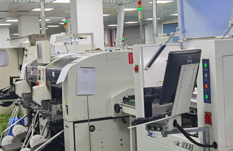
At present, to achieve full automation of perforated printed circuit board installation, it is necessary to expand the area of the original printed circuit board by 40%, so that the automatic plug-in plug-in head can insert the components, otherwise there will be insufficient space and gap, which will damage the components. The automatic placement machine uses a vacuum nozzle to suck and place components. The vacuum nozzle is smaller than the component shape, which can increase the installation density. In fact, small components and fine-pitch QFP components are all produced by automatic placement machines to achieve full-line automated production.
Of course, there are also some problems in SMT mass production. For example, the nominal values on the components are unclear, which makes maintenance difficult and requires special tools; multi-pin QFP is prone to pin deformation and welding failure; the thermal expansion coefficient between components and printed circuit boards is inconsistent, and the solder joints are subjected to expansion stress when the electronic equipment is working, causing the solder joints to fail; in addition, the overall heating of components during reflow soldering will also cause the devices to be subjected to thermal stress, which reduces the long-term reliability of electronic products. However, these problems are all developing problems. With the emergence of special disassembly and assembly equipment and the emergence of new low-expansion coefficient printed circuit boards, they are no longer obstacles to the in-depth development of SMT.
Tags: SMT /surface_assembly_technology /
Prev: Why has FCT replaced ICT in PCBA testing become a trend?
Next: What are the certifications for PCBA processing factories?


