Reflow soldering common quality defects and solutions
Reflow soldering common quality defects and solutions
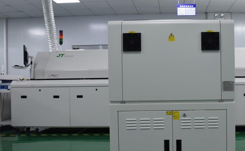
The quality of reflow soldering is affected by a number of factors, the most important factor is the electronic production and processing of reflow furnace temperature profile and the composition of the solder paste Jane number. Now commonly used high-performance reflow furnace, has been relatively easy to accurately control, adjust the temperature profile, in contrast, in the high-density and miniaturization trend, the printing of solder paste has become the key to reflow quality, solder paste, templates and printing of the three factors can affect the quality of solder paste printing.
1, monument phenomenon
Reflow soldering, chip components often stand up the phenomenon known as the monument, also known as the drawbridge, Manhattan phenomenon which is a defect that often occurs in the reflow soldering process.
Causes: The root cause of the phenomenon is the imbalance of the wetting force on both sides of the component, and thus the moment on both sides of the component is also unbalanced, which leads to the occurrence of the phenomenon of the monument.
The following circumstances will lead to reflow soldering components on both sides of the wetting force imbalance.
1, the pad design and layout is unreasonable.
If the pad design and layout of the following defects, will cause components on both sides of the wetting force imbalance.
Components on both sides of one of the pads connected to the ground or one side of the pad area is too large, uneven heat capacity at both ends of the pads
PCB surface of the temperature difference is too large so that the component pads on both sides of the heat absorption is not uniform;
Large devices QFP, BGA, heat sinks around the small piece of component pads at both ends will be uneven temperature phenomenon.
Solution: improve pad design and layout
2, solder paste and solder paste printing.
Solder paste activity is not high or poor solderability of components, solder paste melting, the surface tension is not the same, the same will cause unbalanced pad wetting force. Two pads of solder paste printing is not uniform, more than one side of the solder paste will be due to increased heat absorption, melting time lag, so that the wetting force is not balanced.
Solution: Select the higher activity of the solder paste, improve the solder paste printing parameters, especially the window size of the template.
3, patch.
Z-axis direction of the force is not uniform, will lead to components immersed in the depth of the solder paste is not uniform, melting will be due to the time difference between the two sides of the wetting force is not balanced. Component deviation from the pad will directly lead to the standing monument.
Solution: Adjust the process parameters of the mounter.
4, furnace temperature curve.
PCB heating work curve is not correct, so that the temperature difference on the board is too large, usually reflow oven furnace body is too short and too few temperature zones will appear these defects.
Solution: According to each product to adjust the appropriate temperature profile.
5, N2 reflow soldering in the oxygen concentration.
The use of N2 protection reflow soldering will increase the wetting power of the solder, but more and more reports indicate that the oxygen content is too low in the case of the phenomenon of monumental instead of increasing; it is generally believed that the oxygen content control in (100-500) × 10-6mg/m3 or so the most appropriate.
2, tin beads
Tin bead is one of the common defects of reflow soldering, the cause is multifaceted, not only affects the appearance and will cause bridging.
Tin beads can be divided into two categories, one appears on the side of the chip components, often a large independent ball; the other appears in the IC pins around, scattered small beads.
1, the temperature curve is not correct.
Reflow profile can be divided into four zones, respectively, preheating, holding, reflow and cooling. Preheating, insulation is designed to make the PCB surface temperature in 60-90s to 150 ℃, and insulation of about 90s, which not only reduces the thermal shock of the PCB and components, more importantly, to ensure that the solvent of the solder paste can be partially volatile, to avoid reflow soldering due to too much solvent caused by the splash, resulting in the formation of solder paste rushed out of the pad and the formation of tin beads.
Solution: pay attention to the rate of heating, and take moderate preheating to make a good platform to make most of the solvent volatile.
2, the quality of solder paste.
Solder paste in the metal content is usually (90 ± 0.5) %, metal content is too low will lead to too much flux components, so too much flux will not be easy to evaporate due to preheating stage caused by flying beads.
Increased water vapor and oxygen content in the solder paste can also cause flying beads. Since solder paste is usually refrigerated, when it is taken out of the refrigerator, recovery time is not ensured, so it can lead to the entry of water vapor; in addition, the lid of the solder paste bottle should be tightened after each use, and if the lid is not tightened in time, it can also lead to the entry of water vapor.
Put on the template printed solder paste after the completion of the remaining part should be dealt with separately, if put back into the original bottle, will cause the bottle of solder paste deterioration, but also produce tin beads.
Solution: Choose high-quality solder paste, pay attention to the storage and use of solder paste requirements.
3, printing and patch
In the solder paste printing process, due to the template and pad alignment will occur offset, if the offset is too large will lead to the solder dip flow to the pad outside, easy to appear after heating tin beads. In addition, the printing environment is not good will also lead to the generation of tin beads, the ideal printing environment temperature (25 ± 3) ℃, relative humidity of 50% ~ 65%.
Solution: carefully adjust the clamping of the template to prevent loosening; improve the printing environment.
Patch the process of Z-axis pressure is also an important cause of tin beads, often not easy to cause people to pay attention to, part of the patch machine Z-axis head is based on the thickness of the components to position, such as the Z-axis height is not properly adjusted, it will cause components pasted to the PCB on the moment the solder paste will be extruded outside the pad of the phenomenon, this part of the solder paste will be formed in the welding of tin beads. This part of the solder paste will form a bead when soldering. The size of the bead produced in this case is slightly larger.
Solution:Re-adjust the height of the Z-axis of the mounter.
Stencil thickness and opening size. Excessive stencil thickness and opening dimensions can lead to increased solder paste usage and can cause solder paste to flow outside the pads, especially with chemically etched stencils.
Solution: Select the appropriate thickness of the template and the opening size of the design, the general template opening area of 90% of the size of the pad, will improve the situation of tin beads.
4, core suction phenomenon
Core suction phenomenon, also known as the core phenomenon, is one of the common welding defects, mostly found in gas-phase reflow soldering. Core suction phenomenon is the solder out of the pad and along the pins up to the pins and chips between the body, usually forming a serious phenomenon of virtual welding.
Causes.
The main reason is that the thermal conductivity of the component pins, so the temperature rises rapidly, so that the solder priority wetting pins, solder and the wetting force between the pins is much larger than the wetting force between the solder and the pad In addition, the pin's upward warping will exacerbate the occurrence of the phenomenon of core suction.
Solution.
For gas-phase reflow soldering, the SMA should first be fully preheated before placing it in the gas-phase oven;
The solderability of PCB pads should be carefully checked, and PCBs with poor solderability should not be used in production;
Pay full attention to the co-planarity of the components, and the devices with bad co-planarity are not applied to the production.
In the infrared reflow soldering, PCB substrate and solder in the organic flux is a good infrared absorption medium, while the pins can partially reflect infrared, so compared to the solder priority melting, solder and pad wetting force will be greater than the wetting force between the solder and the pins, so the solder will not be along the pins rise, so the probability of core suction phenomenon is much smaller.
5, bridging
Bridging is one of the common defects in the production of SMT, it will cause a short circuit between components, encountered bridging must be repaired.
Caused by a number of reasons for bridging, the following four common.
1, solder paste quality problems.
Solder paste metal content is high, especially after printing time is too long, easy to increase the metal content, resulting in IC pin bridging;
Solder paste viscosity is low, after preheating diffuse to the outside of the pad;
Poor solder paste collapse, after preheating the diffuse flow to the outside of the pad.
Solution: adjust the ratio of solder paste or switch to a good quality solder paste.
2, printing system.
Poor repeatability of the printing machine, alignment is not aligned (steel plate alignment is not good, PCB alignment is not good), resulting in the printing of solder paste to the pad outside, mostly in the production of fine-pitch QFP;
Steel plate window size and thickness design is not right, as well as PCB pad design Sn-Pb alloy coating is not uniform, resulting in excessive amount of solder paste.
Solution:Adjust the printing machine to improve the PCB pad coating layer.
3, paste and put.
Placement pressure is too high, the solder paste is pressurized by the diffuse flow is a common cause in production. In addition, the placement accuracy is not enough, the components are shifted, IC pin deformation, etc. also easily lead to bridging.
4, preheating.
Reflow oven heating speed is too fast, the solvent in the solder paste to volatilize.
Solution: Adjust the height of the Z-axis of the mounter and reflow furnace heating speed.
Tags: solutions /
Prev: PCBA fast sampling process
Next: PCBA processing is not equal to the "low-end manufacturing"


