
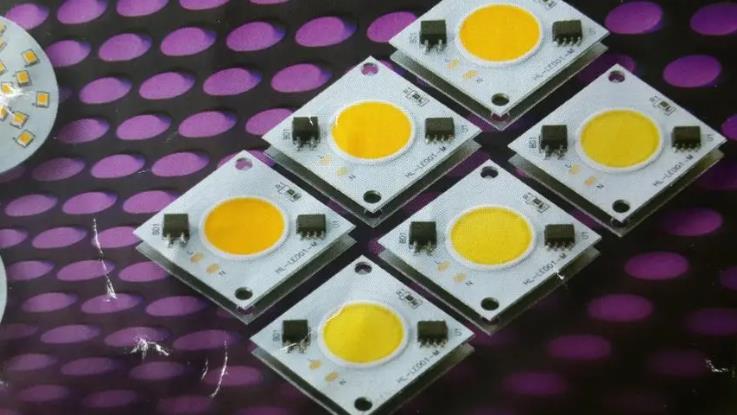
LED PCB board design and manufacturing process and difficulties
The design and manufacturing process of LED PCB boards involves several key steps, along with some challenges that need to be addressed. Here is a detailed overview:
Design Process:
- Requirement Analysis and Specification: The initial step involves understanding the specific requirements and specifications of the LED PCB board, such as size, layout, power handling, and thermal considerations.
- Schematic Capture: Using CAD software, the electrical circuit is designed and captured in the form of a schematic diagram.
- PCB Layout: The schematic diagram is then converted into a PCB layout, taking into account component placement, routing of traces, and the overall board size. Parameters like adjacent wire spacing, minimum spacing, and pad-to-board edge distance are carefully considered to ensure electrical safety and manufacturability.
- Verification and Simulation: The PCB layout is verified for correctness and simulated to check for potential issues like signal integrity, electromagnetic compatibility, and thermal performance.
- Gerber File Generation: Once the layout is finalized, it is converted into Gerber files, which are used by manufacturing equipment for PCB production.
Manufacturing Process:
- Material Selection: The choice of materials, including the base material, copper thickness, and surface finish, is critical to the PCB's performance and reliability.
- Fabrication: The PCB is fabricated using processes like etching, drilling, and cutting, based on the Gerber files.
- Component Placement and Soldering: Components are precisely placed on the PCB using automated machines, followed by soldering to establish electrical connections.
- Inspection and Testing: The finished PCB is inspected for defects and tested for electrical performance and reliability.
Key Challenges:
- Material Selection: Choosing the right materials for the PCB is crucial, considering factors like conductivity, insulation, temperature resistance, and corrosion resistance.
- Layout Optimization: Achieving an optimal layout that ensures signal integrity, reduces noise, and allows for efficient heat dissipation can be challenging.
- Soldering Quality: Ensuring high-quality soldering is essential for reliable electrical connections. Controlling soldering parameters like temperature, time, and pressure is critical.
- Quality Control: Implementing a robust quality control system to detect and correct defects during and after manufacturing is important to ensure product quality.
LED PCB board design and manufacturing is a complex process that requires careful consideration of multiple factors. By addressing the key challenges and leveraging advanced tools and techniques, manufacturers can produce high-quality LED PCB boards that meet the demanding requirements of modern LED applications.
Tags: PCB /manufacturing /design /LED /LED_PCB_board /
Prev: Can Vietnam overtake China in PCBA manufacturing?
Next: Process requirements for DIP plug-in


