
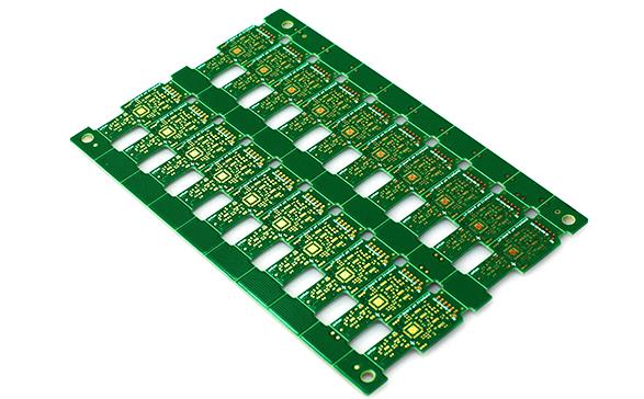
Two common PCB panel designs
Two common PCB panel designs
1. V-groove panel design
The V-groove panel connection method is suitable for panels with a thickness of ≥1.0mm and straight edges of the PCB (sub-board). PCBs with a thickness of <1.0mm are not suitable for V-groove paneling because the thinner the PCB, the smaller the depth of the V-groove, and it is difficult to insert the groove when using a rotary knife to separate the panels. When manually separating the panels, the stress is not concentrated, the entire board will bend, and components are easily damaged.
Design requirements:
(1) The general design requirements for the shape and size of the V-groove are as follows:
The residual thickness is generally 1/3 of the board thickness, with a minimum of 0.40mm;
The angle of the V-groove is 30°~45°, with 30° recommended;
The misalignment of the cuts on the upper and lower sides of the V-groove should be <0.13mm
(2) The height limit of components on both sides of the V-groove: within 5mm from the V-groove, the component height is <27mm; within 5~20mm from the V-groove, the component height is <35mm.
(3) The wire or copper sheet should be more than 1.0mm away from the edge of the V-groove to avoid damaging the conductor during board separation.
Note:
The residual thickness of the V-groove processing should be determined according to the board thickness to ensure good board separation and welding. If stress-sensitive components (such as chip capacitors, BGA, etc.) are installed on the unit PCB, it is not recommended to use manual board separation, and machine board separation should be used.
There are two types of V-groove splitters, namely front and back feeding (2M) and left and right feeding (4M). The former has PCB movement, which is prone to board cutting deviation and poor stress stability; the latter has PCB immobility and better processability.
The strain direction of V-groove manual splitting is perpendicular to the V-groove direction, while the strain direction of machine splitting is mostly 30°~45° to the V-groove direction, so the requirements for component layout direction are different.
2. Stamp hole panel design
The stamp hole panel connection method, that is, the connection method of long slot plus stamp hole, is used for panelization of various sub-boards. Its design parameters mainly include the size of the long slot and the stamp hole diameter and spacing.
Design requirements:
(1) The slot width is generally 1.6~3.0mm, with a recommended value of 2.4mm; the slot length should be ≤50mm; the width of the connecting bridge between slots is designed according to the required size of 5 holes or 7 holes.
(2) The diameter of the stamp hole is Ø0.8mm; the center distance of the hole is generally the diameter plus 0.4mm~0.6mm. The smaller value is used for thicker boards and the larger value is used for thinner boards.
(3) The semicircles at both ends of the long slot are tangent to or connected to the stamp hole.
(4) The maximum distance between the connecting bridge and the corner is 12.5mm.
(5) The wire or copper sheet should be more than 1.5mm away from the edge of the stamp hole to avoid damaging the conductor during board separation.
Note:
The stamp hole connection method is a more commonly used panel connection method, suitable for PCBs with regular and irregular shapes.
With the increase in component layout density, the layout of components is getting closer and closer to the dividing edge. In order to avoid stress damage to nearby components during board separation, a mechanical milling board separation process is used. In this case, the existence of the stamp hole is meaningless, thus deriving the long slot hole connection method, which has high connection strength and is widely used in thin board panel design. The disadvantage is that a special milling board separation machine is required for board separation.
Prev: What is the difference between SMD and SMT? How to choose an SMT factory?
Next: PCBA Metallization Board Edge Considerations


