
PCBA Metallization Board Edge Considerations
In the PCBA manufacturing process, metallized board edges are an important link, and their quality directly affects the overall performance and reliability of PCBA. Here are some things to note about PCBA metallized board edges:
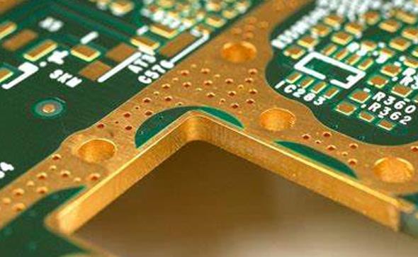
I. Metallization Edge Design
- Connectivity Design:
- Ensure that the metallized edge has proper connections with the inner layers of the PCB to prevent delamination or shedding of the metal edge during soldering. This is crucial because without inner layer connections, the metallized edge can separate from the PCB substrate due to stress or temperature changes during soldering.
Pay special attention to the metallization design in areas with large-sized vias or holes to ensure the metal layer remains firmly attached to the PCB.
II. Metallization Process
- Cleaning:
- Thoroughly clean the PCB surface before metallization to remove dirt, grease, and other impurities, ensuring that the metal layer can adhere evenly and firmly to the PCB.
- Metallization Methods:
- Choose metallization methods such as immersion plating, spraying, etc., based on specific application requirements and PCB material.
- Baking and Cooling:
- After metallization, bake the PCB to ensure that the metal layer adheres uniformly and firmly. Follow up with proper cooling to prevent PCB damage due to temperature changes.
III. Quality Control
- Inspection and Testing:
- Conduct rigorous inspections and tests after the metallization process to ensure the metallization layer meets quality requirements. This includes checking adhesion, uniformity, conductivity, and other performance indicators.
- Environmental Control:
- Strictly control the production environment throughout the metallization process, including temperature, humidity, and cleanliness, to ensure process stability and reliability.
IV. Other Precautions
- Avoid Stacking:
- During PCBA processing, avoid stacking circuit boards to prevent physical wear and cross-contamination between boards.
- Static Electricity Prevention:
- As static electricity poses significant hazards to electronic components, wear electrostatic clothing, shoes, and other protective gear when handling circuit boards to prevent electrostatic interference.
- Operational Norms:
- Processing personnel must strictly adhere to operational norms to avoid damaging PCBAs through incorrect handling methods. For example, avoid touching the surface of soldered PCBAs with bare hands, as human oils can affect solderability.
By strictly adhering to these precautions, the quality and reliability of PCBA metallization edges can be ensured.
Tags: PCBA /Metallization /Considerations /
Prev: Two common PCB panel designs
Next: High-Speed Printed Circuit Board Manufacturing and Assembly


