
PCB Assembly Service ODM Process
The PCB Assembly Service ODM (Original Design Manufacturer) outsourcing process is a complex yet meticulous endeavor, encompassing various stages from design, procurement, production, to testing, packaging, and shipment. Here's a detailed overview of the process :
1. Customer Needs Analysis and Evaluation
Communication: The ODM service provider first engages in thorough communication with the client to clarify requirements and expectations, including product functionality, performance metrics, production quantity, and lead time.
Project Assessment: Based on the client's input, the service provider evaluates the project's feasibility and cost-effectiveness to ensure a smooth execution.
2. Design and Development
PCB Design: Electronic engineers utilize specialized EDA (Electronic Design Automation) software to create PCB layouts based on schematic diagrams, optimizing layout and routing for electrical performance, thermal management, and signal integrity.
Design Review: Upon completion, the design undergoes internal or client-participated reviews to validate its compliance with requirements and optimize the solution.
3. Material Procurement
BOM Compilation: A detailed procurement plan is formulated based on the design requirements and BOM (Bill of Materials).
Supplier Selection: Reliable suppliers are selected for sourcing electronic components and PCB boards.
Incoming Inspection: All procured materials undergo rigorous quality inspections to ensure compliance with production standards.
4. PCB Fabrication
Manufacturing Process: The PCB boards are produced through processes such as panel cutting, drilling, plating, and etching to meet design specifications.
Quality Control: Completed PCBs are subjected to stringent quality checks to ensure conformity with production standards.
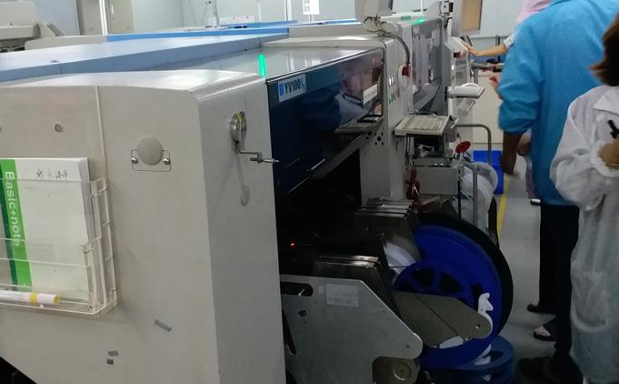
5. Component Placement and Through-hole Insertion
SMT Mounting: Automated equipment precisely places surface-mount components on the PCB, followed by reflow soldering for secure attachment.
DIP Insertion: Components with long leads are inserted into PCB through-holes and soldered using wave soldering or other methods to ensure robust connections.
6. Product Testing and Inspection
Functional Testing: Electrical performance tests are conducted to verify product functionality.
Reliability Testing: Stress tests like hi-pot, high-temperature aging, etc., ensure product reliability and stability.
Visual Inspection: Products undergo visual checks for flaws and damages.
7. Final Packaging and Shipment
Packaging: Products are appropriately packaged and labeled according to client requirements to ensure safe transportation and storage.
Shipment: Finished goods are dispatched to the client at the agreed time and location.
8. After-Sales Service and Support
Technical Support: Provides troubleshooting and repair services for technical issues encountered during product usage.
Quality Traceability: Establishes a quality traceability system to track and resolve issues.
By following this comprehensive process, ODM service providers deliver high-quality, efficient PCB Assembly services tailored to clients' diverse needs. Continuous process optimization, technological advancements, and service quality enhancements are crucial for maintaining competitiveness in the market.
Tags: PCB /ODM /PCB_Assembly_Service /Process /
Prev: What is SMT in PCB manufacturing?
Next: SMT lead-free process requirements and solutions


