The Difference and Connection Between PCB Layout and PCBA Layout
In the process of electronic product development, PCB Layout and PCBA Layout are two critical stages. While they differ in scope, they are closely interconnected. Understanding their roles helps optimize circuit board design and enhances product performance and reliability.
1. Concepts and Scope
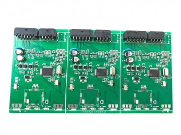
PCB Layout (Printed Circuit Board Layout) focuses on the design of the bare board. Designers consider factors such as board dimensions, the number of layers, and signal routing to ensure the circuit’s electrical performance meets the desired specifications. Essentially, PCB Layout forms the structural framework for subsequent assembly processes.
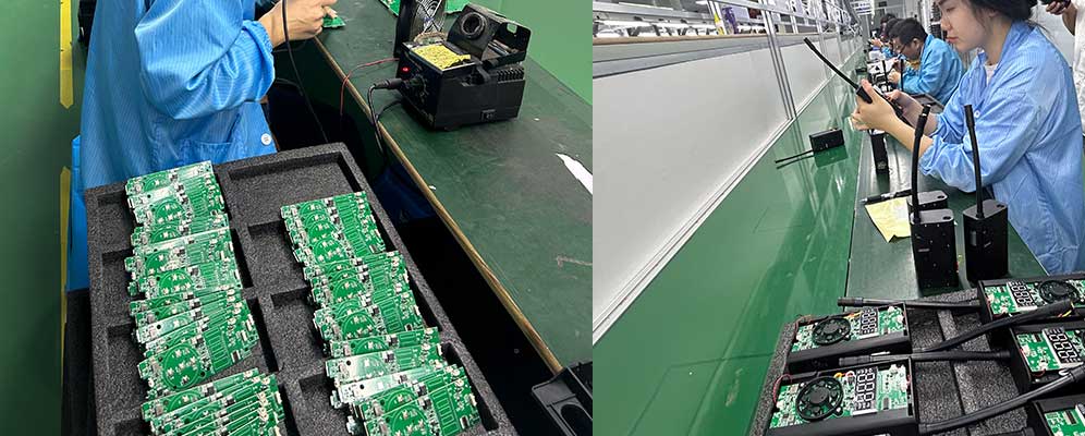
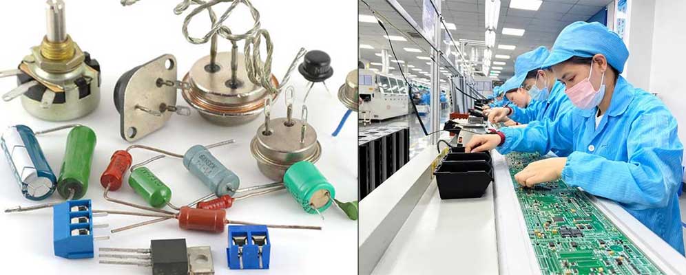
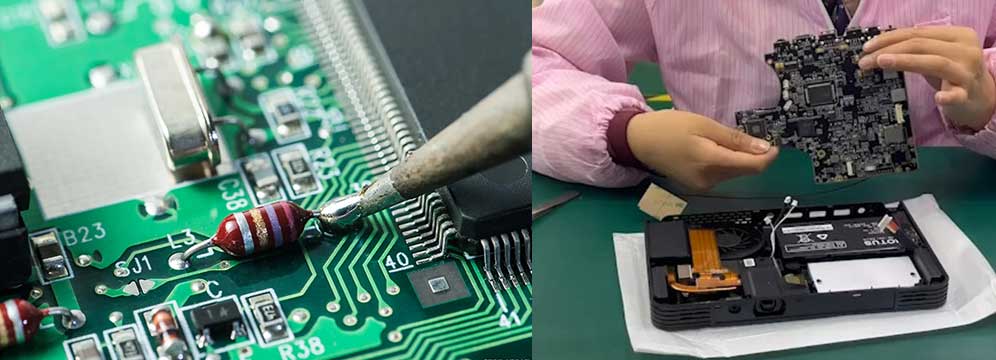
In contrast, PCBA Layout (Printed Circuit Board Assembly Layout) extends beyond PCB Layout. It includes the placement and assembly of electronic components on the board. In addition to electrical performance, PCBA Layout addresses factors like soldering feasibility, thermal management, and mechanical strength to ensure the entire circuit operates efficiently after assembly.
2. Design Priorities
PCB Layout emphasizes optimizing electrical performance, focusing on factors such as signal transmission integrity, impedance matching, and electromagnetic compatibility. Its primary goal is to create a reliable foundation for electrical connectivity.
PCBA Layout, however, focuses more on assembly practicality and overall product reliability. This includes determining optimal component placement for automated production, designing solder pads for efficient soldering, and creating thermal pathways to enhance the product's lifespan.
3. Process Involvement
PCB Layout primarily involves EDA tools (such as Altium Designer or Mentor Graphics) and is concentrated on the circuit design phase.
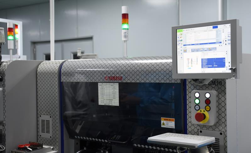
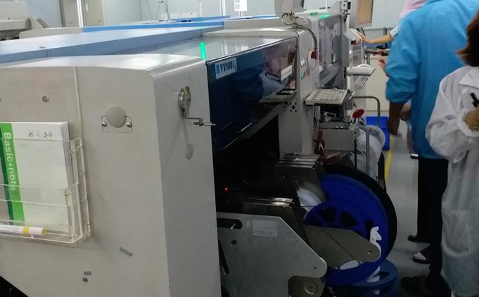
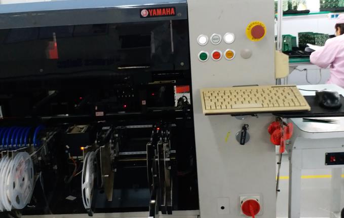
PCBA Layout, on the other hand, is closely tied to manufacturing processes. For instance, it ensures compliance with SMT (Surface Mount Technology) requirements, maintains proper spacing between components, and designs pads that facilitate automated assembly—all of which influence production efficiency and product stability.
4. Purpose and Application
The main goal of PCB Layout is to provide a high-quality foundation for circuit board production and ensure the accurate implementation of circuit designs.
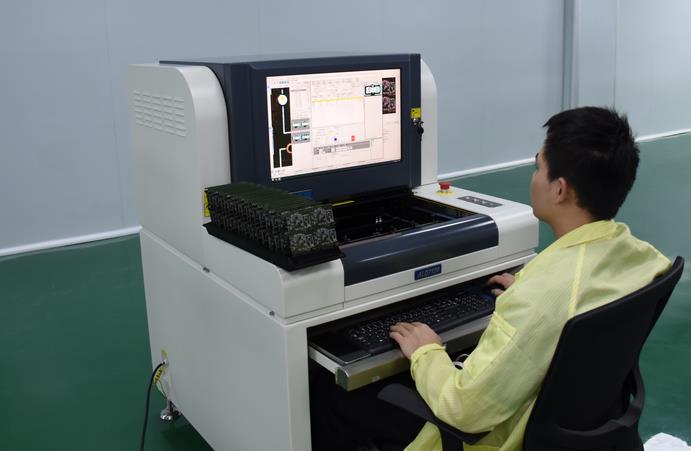
In contrast, PCBA Layout aims to achieve functional and manufacturable circuit boards. This includes the assembly, debugging, and final testing stages, ensuring the product is fully functional and ready for end-user applications.
Conclusion
In summary, PCB Layout focuses on the design of the bare board, serving as the initial stage of the development process. PCBA Layout encompasses the entire workflow, from circuit design to component assembly, ensuring manufacturability and performance. Together, they play an essential role in the development and production of electronic products.
If you're looking for professional PCBA Layout services, we have extensive experience and state-of-the-art equipment to offer a one-stop solution. Whether it's small-batch prototyping or large-scale production, we can customize our services to meet your needs and help your product stand out in the market!
Tags: PCBA /PCB Layout /PCBA Layout /PCB Assembly /
Next: Differences Between PWB, PCB, and PCBA


