
PCBA processing factory teaches you step by step how to copy the board
Simply put, the technical implementation process of PCB copying is to scan the circuit board to be copied, record the detailed component locations, and then remove the components to make a bill of materials (BOM) and arrange material procurement. The empty board is The scanned image is processed by the board copying software and restored into a pcb board diagram file, and then the PCB file is sent to the plate making factory to make the board. After the board is made, the purchased components are welded to the finished PCB board, and then the circuit board is tested. and debugging.
1. Specific steps for PCB copying
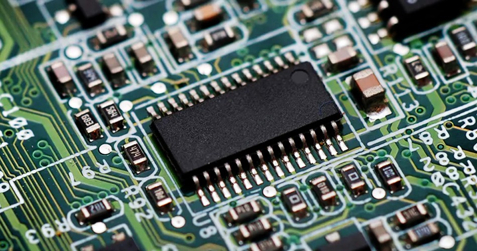
1. Get a PCB, first record the model, parameters, and location of all vitality components on paper, especially the direction of the diode, transistor, and the direction of the IC gap. It is best to take two photos of the location of the vitality piece with a digital camera. Today's PCB circuit boards are becoming more and more advanced. The diodes and transistors on them are almost invisible if you don't pay attention.
2. Remove all multi-layer board components and remove the tin from the PAD holes. Clean the PCB with alcohol and then put it into the scanner. When scanning, the scanner needs to slightly increase the scanning pixels in order to get a clearer image. Then use water gauze paper to lightly polish the top and bottom layers until the copper film shines. Put it in the scanner, start PHOTOSHOP, and scan in the two layers separately in color. Note that the PCB must be placed horizontally and vertically in the scanner, otherwise the scanned image will not be usable.
3. Adjust the contrast and lightness of the canvas so that the part with copper film and the part without copper film have a strong contrast. Then convert the image to black and white and check whether the lines are clear. If not, repeat this step. If it is clear, save the picture as black and white BMP format files TOP.BMP and BOT.BMP. If you find problems with the graphics, you can use PHOTOSHOP to repair and correct them.
4. Convert the two BMP format files to PROTEL format files respectively, and transfer the two layers in PROTEL. If the positions of PAD and VIA after the two layers are basically coincident, it indicates that the first few steps have been done well. If there is a deviation , then repeat step three. Therefore, PCB board copying is a job that requires great patience, because any small problem will affect the quality and matching degree after copying the board.
5. Convert the BMP of the TOP layer to TOP.PCB. Pay attention to convert it to the SILK layer, which is the yellow layer. Then just trace the line on the TOP layer and place the device according to the drawing in the second step. After painting, delete the SILK layer. Repeat until all layers are drawn.
6. Transfer TOP.PCB and BOT.PCB into PROTEL and combine them into one picture.
7. Use a laser printer to print the TOP LAYER and BOTTOM LAYER on transparent film (1:1 ratio), put the film on the PCB, and compare whether there are errors. If they are correct, you are done.
A copy board that is identical to the original board is born, but this is only half the job. Testing is also required to test whether the electronic performance of the copied board is the same as that of the original board. If it's the same, it's really done.
Note: If it is a multi-layer board, you need to carefully polish the inner layer, and repeat the third to fifth steps of copying the board. Of course, the naming of the graphics is also different, depending on the number of layers. Generally, double-sided board copying requires It is much simpler than multi-layer boards. Multi-layer board copying is prone to misalignment, so multi-layer board copying must be particularly careful and careful (the internal conductive holes and non-conductive holes are prone to problems).
2. Double-sided board copying method
1. Scan the upper and lower surfaces of the circuit board and save two BMP pictures.
2. Open the board copying software Quickpcb2005, click "File" and "Open Base Image" to open a scanned image. Use PAGEUP to enlarge the screen, see the pads, press PP to place a pad, and press PT to route the lines... just like a child tracing a picture, trace it in this software, and click "Save" to generate a B2P file.
3. Then click "File" and "Open Base Image" to open the scanned color image of another layer.
4. Click "File" and "Open" again to open the B2P file saved earlier. We see the board we just copied, superimposed on this picture - the same PCB board, the holes are in the same position, but the circuit connections are different. . So we press "Options" - "Layer Settings" and turn off the display of top-level lines and silkscreens here, leaving only multi-layer vias.
5. The via holes on the top layer are at the same position as the via holes on the bottom layer picture. Now we can just trace the circuit on the bottom layer like we traced in childhood. Click "Save" again - the B2P file now has two layers of data: the top layer and the bottom layer.
6. Click "File" and "Export as PCB file" to get a PCB file with two layers of data. You can then modify the board or produce a schematic diagram or directly send it to a PCB plate making factory for production.
In fact, four-layer board copying means copying two double-sided boards repeatedly, and six-layer board copying means repeating three double-sided boards... The reason why multi-layer boards are daunting is that we cannot see the internal wiring. How can we see the inner world of a sophisticated multi-layer board? ——Layering.
Nowadays, there are many ways to layer layers, such as chemical corrosion, knife peeling, etc., but it is easy to over-separate the layers and lose data. Experience tells us that sandpaper is the most accurate.
After we copy the top and bottom layers of the PCB, we usually use sandpaper to remove the surface layer and reveal the inner layer. The sandpaper is ordinary sandpaper sold in hardware stores. Generally, the PCB is laid flat, and then the sandpaper is pressed and rubbed evenly on the PCB. (If the board is small, you can also lay the sandpaper flat and hold down the PCB with one finger and rub it on the sandpaper). The key is to lay it flat so that it can be ground evenly.
Silk screen printing and green oil usually come off with just a wipe, but copper wires and copper sheets need to be wiped carefully several times. Generally speaking, a Bluetooth board can be wiped in a few minutes, and a memory module can be wiped in about ten minutes. Of course, if you have more effort, it will take less time; if you have less effort, it will take more time.
Grinding boards is currently the most commonly used solution for layering and is also the most economical. We can find a discarded PCB and try it. In fact, there is no technical difficulty in grinding the board, but it is a bit boring and requires some effort. There is no need to worry about grinding the board to your fingers.
During the PCB layout process, after the system layout is completed, the PCB drawing must be reviewed to see whether the system layout is reasonable and whether it can achieve optimal results.
It can usually be investigated from the following aspects:
1. Whether the system layout ensures reasonable or optimal wiring, reliable wiring, and reliable circuit operation. When laying out, you need to have an overall understanding and planning of the signal direction and the power and ground network.
2. Whether the size of the printed board matches the size of the processing drawing, whether it meets the PCB manufacturing process requirements, and whether there are behavioral marks. This point requires special attention. The circuit layout and wiring of many PCB boards are designed beautifully and reasonably, but the precise positioning of the connectors is neglected, resulting in the designed circuit being unable to connect with other circuits.
3. Whether the components conflict in two-dimensional or three-dimensional space. Pay attention to the physical dimensions of the device, especially the height of the device. When soldering layout-free components, the height generally cannot exceed 3mm.
4. Whether the component layout is dense and orderly, neatly arranged, and whether all components have been laid out. When laying out components, we must not only consider the direction and type of signals, and areas that need attention or protection, but also consider the overall density of the device layout to ensure uniform density.
5. Can components that need to be replaced easily be replaced, and whether plug-in boards can be easily inserted into the equipment. The replacement and connection of frequently replaced components should be ensured to be convenient and reliable.
Tags: PCBA /copy /factory /board /teaches /
Prev: What is PCBA? What is the difference between PCBA and PCB?
Next: The difference between laser welding and reflow soldering in PCBA processing


