PCB assembly factory answers for you: What are the components of a circuit board?
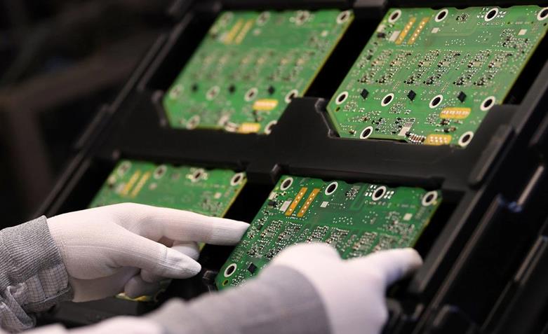
The era of the Internet of Things is filled with intelligent electronic products, and circuit boards are the core component of electronic products. Now let's understand what components circuit boards have:
1. Pads:
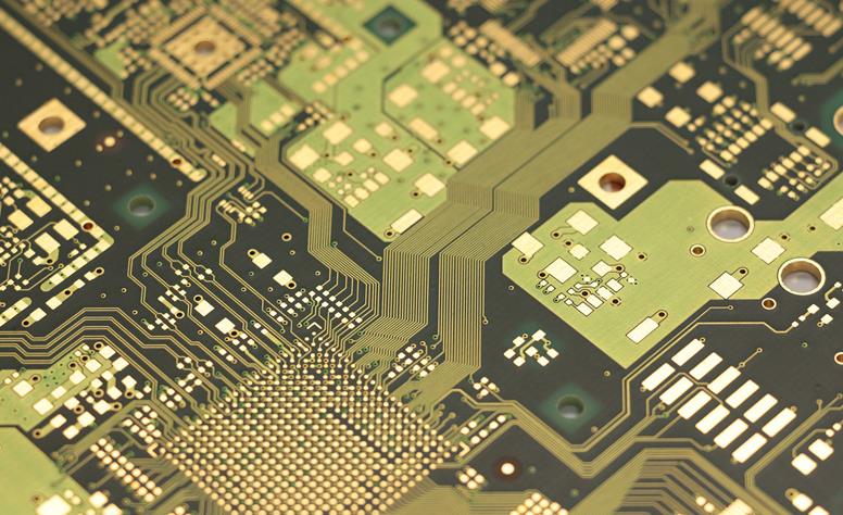
A solder pad is a metal hole used to solder the pins of a component.
2. Layer:
According to different designs, circuit boards may have double-sided boards, 4-layer boards, 6-layer boards, 8-layer boards, etc. The number of layers is usually even. In addition to the layers for signal transmission, there are other layers used to define processing.
3. Through hole:
The meaning of via is that if the circuit cannot achieve all signal routing on one level, the signal lines need to be connected across layers through via. There are generally two types of via: metal via and non-metal via, where metal via is used to connect component pins between layers. The form and aperture of the through-hole depend on the characteristics of the signal and the requirements of the processing plant's process.

4. Components:
The wiring combination between different components soldered onto the PCB board can achieve different functions, which is also the role of the PCB.
5. Wiring:
Wiring refers to the signal line between the pins of a connector, and the length and width of the wiring depend on the nature of the signal, such as current magnitude, speed, etc. The length and width of the wiring also vary.
6. Screen printing:
Silk screen, also known as silk screen layer, is used to label various relevant information on devices. Silk screen is generally white, and colors can be selected according to personal needs.
7. Solder resistance layer:
The main function of the solder mask layer is to protect the surface of the PCB, form a protective layer with a certain thickness, and block the contact between copper and air. The solder mask layer is generally green, but there are also options for red, yellow, blue, white, and black solder mask layers.
8. Positioning hole:
Positioning holes are holes designed for easy placement during installation or debugging.
9. Fill:
Filling is used for copper deposition in the ground wire network, which can effectively reduce impedance.
10. Electrical boundary:
The electrical boundary is used to determine the size of a circuit board, and all components on the circuit board must not exceed this boundary.
The above ten parts are the foundation of the circuit board, and the implementation of more functions still needs to be achieved by burning programs in the chip.
Tags: factory /circuit_board /PCB_assembly /
Next: Why is the PCB circuit board green?


