
Frequently Asked Questions
Organize common question answers to answer your questions and clarify your doubts
1. What should be noted when making PCBA cross-border samples?
PCBA cross-border sampling is a complex process involving multiple links and factors. To ensure the smooth progress of sampling and product quality, the following are some things to pay attention to:
1、 Choose the appropriate PCB manufacturer
Technical strength: Choose PCB manufacturers with advanced technology and rich experience to ensure that high-quality circuit boards can be produced according to design requirements.
Production capacity: Consider the manufacturer's production scale and capacity to ensure timely delivery of sample products.
Quality control: Understand the manufacturer's quality control system to ensure that products meet quality requirements.
Reputation and word-of-mouth: By conducting online searches, consulting with peers, and other means, we can understand the reputation and word-of-mouth of manufacturers and choose reputable ones for cooperation.
2、 Confirm circuit diagram design
Design rationality: Before cross-border sampling, it is necessary to confirm whether the circuit diagram design is reasonable, including circuit schematic, PCB layout, component list, and other aspects.
Compatibility: Consider electrical standards and specifications from different countries and regions to ensure that circuit designs meet the requirements of the target market.
3、 Component procurement
Model and specifications: Confirm whether the model and specifications of the components used are correct, and consider the supply situation of components in different countries and regions.
Performance and characteristics: Understand the performance and characteristics of components to ensure compliance with design requirements.
Supplier selection: Choose reliable component suppliers to ensure the quality and supply stability of the components.
4、 PCB process flow
Board selection: Select appropriate PCB boards according to design requirements to ensure the performance and reliability of the circuit board.
Printing process: Understand the different steps of PCB printing process, such as photolithography, etching, metalization, etc., and choose the suitable process flow for the target market.
Surface treatment process: Select appropriate PCB surface treatment processes according to design requirements, such as electroplating, tin spraying, hot air leveling, etc.
5、 Quality control
Raw material procurement: Select high-quality raw material suppliers and strictly control their quality.
Production process monitoring: Real time monitoring and recording of the production process to promptly identify and resolve issues.
Quality inspection and testing: Conduct strict quality inspection and testing on PCBA products to ensure that they meet design requirements and quality standards.
6、 Communication and feedback
Strengthen communication and feedback between the design team, manufacturer, and testing team to ensure timely transmission of information and resolution of issues.
Promptly identify problems and provide feedback to the design team, optimize and improve them accordingly to improve the performance and quality of the circuit board.
7、 Logistics and Delivery
Choose a reliable logistics company for cross-border transportation to ensure timely delivery and good condition of products.
During the delivery process, pay attention to the packaging and protection of the product to ensure that it is not damaged during transportation.
8、 Legal regulations and standards
Understand and comply with the laws, regulations, and standards of the target market to ensure that the product meets the requirements of the local market.
Pay attention to intellectual property issues and ensure that the intellectual property rights of others are not infringed upon during the cross-border sampling process.
PCBA cross-border sampling requires attention to multiple aspects, including selecting a suitable PCB manufacturer, confirming circuit diagram design, component procurement, PCB process flow, quality control, communication and feedback, logistics and delivery, as well as laws, regulations and standards. Only by comprehensively considering these issues and taking corresponding measures can we ensure the smooth progress of PCBA cross-border sampling and product quality.
2. What is the largest PCB company in the world?
The largest PCB company in the world is Pengding Holding (鹏鼎控股). This company is a member of the Zhen Ding Technology Group and is based in Taiwan. Key points about Pengding Holding include:
Revenue: In April 2024, Pengding Holding achieved a revenue of NT$110.57 billion, representing a year-on-year increase of 54.9%.
Products: The company offers a diverse range of PCB products, including FPC, SMA, SLP, HDI, MiniLED, RPCB, and RigidFlex, which are widely used in communication electronics, consumer electronics, computers, automobiles, and AI servers.
Market Position: According to Prismark's global PCB enterprise ranking based on revenue from 2018 to 2024, Pengding Holding has been the world's largest PCB manufacturer for seven consecutive years from 2017 to 2023.
Customers: Pengding Holding is a core supplier to brands such as Apple, Huawei, OPPO, vivo, and Google, and is deeply involved in the early-stage research and development of customer products.
In summary, Pengding Holding's significant revenue growth, diverse product line, and leading market position make it the largest PCB company in the world.
3. Can the number of PCB assembly manufacturers in a country reflect its industrial strength?
The number of PCB assembly manufacturers in a country can serve as an indicator of its industrial strength, but it should be considered in the context of several other factors. Here are some key points to consider:
Manufacturer Density and Concentration:
- If a country has a high density of PCB assembly manufacturers, especially in specific regions like the Pearl River Delta (PRD) or Yangtze River Delta (YRD) in China, it suggests a developed and concentrated PCB industry. This concentration often leads to better supply chain management, lower costs, and improved efficiency.
Technical Capabilities and Expertise:
- The number of manufacturers alone does not fully reflect the technical capabilities of a country's PCB industry. However, a large number of manufacturers may indicate a wider range of technological expertise and capabilities, including the ability to handle complex designs, use advanced materials, and employ automated and high-precision assembly techniques.
Market Share and Competitiveness:
- A country with a large number of PCB assembly manufacturers may have a significant share in the global PCB market. This can indicate competitiveness and the ability to meet demand from a wide range of customers and industries. However, market share alone does not fully represent the industrial strength, as other factors like product quality, innovation, and brand reputation also play important roles.
Industry Policies and Support:
- Government policies and support for the PCB industry can significantly influence its development and strength. A country with a favorable policy environment, including tax incentives, research funding, and trade agreements, is likely to attract more manufacturers and investments, leading to a stronger PCB industry.
Supply Chain Integration and Collaboration:
- A robust PCB industry often involves close collaboration and integration within the supply chain. This includes relationships between PCB manufacturers, component suppliers, equipment providers, and end-customers. A country with a well-developed supply chain ecosystem and strong collaboration among stakeholders is likely to have a more competitive and resilient PCB industry.
While the number of PCB assembly manufacturers in a country can provide a rough indication of its industrial strength, a more comprehensive assessment should consider factors like technical capabilities, market share, policies, and supply chain integration.
4. What are the components and configurations of a typical 4-layer PCB stack?
In a typical 4-layer PCB (Printed Circuit Board) stack-up, the number of layers depends on the complexity and specific requirements of the circuit design. While not all PCBs strictly have 4 layers, a typical 4-layer PCB stack-up might include the following types of layers:
- Top Layer:
- This is one of the outer layers of the PCB and is typically used for placing components (such as integrated circuits, resistors, capacitors, etc.) and their connecting traces.
- The top layer may also contain pads (Pads) for soldering components and vias (Vias) for connecting to internal or bottom layer circuitry.
- Inner Layer 1:
- This is one of the internal layers of the PCB and is used to connect the circuitry between the top and bottom layers.
- The inner layer typically contains signal lines (Signal Lines) that transmit data and instructions.
- In a multilayer PCB, the inner layer may also include power and ground planes to provide power distribution and grounding connections.
- Inner Layer 2:
- This is another internal layer, similar to Inner Layer 1, and it is used to further expand the connectivity and routing of the circuitry.
- It can contain additional signal lines, power, and ground planes to meet the needs of more complex circuit designs.
- Bottom Layer:
- This is the other outer layer of the PCB, opposite to the top layer.
- The bottom layer can also be used for placing components and their connecting traces, but usually with a lower component count, for specific needs or space constraints.
- The bottom layer also contains pads and vias for connecting to other layers or external circuitry.
It is important to note that this is a typical example of a 4-layer PCB stack-up. In reality, PCBs can range from single-layer to dozens of layers, depending on the demands and complexity of the circuit design. Additionally, the design of the PCB stack-up needs to consider other factors such as electromagnetic compatibility (EMC), thermal management, signal integrity, and cost-effectiveness.
5. What is the difference between SMT and THT?
SMT (Surface Mounted Technology) and THT (Through-Hole Technology) are two different approaches in electronic assembly and soldering. Here are the key differences between the two:
Component Attachment Method:
- SMT: Components are attached directly to the surface of the printed circuit board (PCB) without passing through holes. The components are typically smaller in size with short leads or no leads at all.
- THT: Components are attached by inserting their leads or pins through holes drilled in the PCB. The leads are then soldered on the opposite side of the PCB, creating a mechanical and electrical connection.
Soldering Technique:
- SMT: Uses surface mount soldering techniques such as reflow soldering or wave soldering in some cases, where the solder paste is applied to the PCB pads before the components are placed. The solder paste is then melted to create the connection.
- THT: Uses wave soldering primarily, where the PCB with inserted components is passed over a wave of molten solder, contacting and bonding the component leads to the PCB pads.
Application and Characteristics:
- SMT: Ideal for high-density PCBs and compact designs. Provides excellent electrical performance, high reliability, and is suitable for automated production lines. SMT components are typically smaller and lighter, making the final product more compact.
- THT: More suitable for larger components with longer leads or pins. Provides a secure physical connection and better heat dissipation. However, THT components tend to be larger and heavier, limiting the overall density of the PCB.
Cost and Efficiency:
- SMT: Tends to be more cost-effective for high-volume production due to its high degree of automation and smaller component sizes.
- THT: May be more suitable for low-volume or prototype production, as manual soldering is often required. However, the overall cost per component may be higher due to the larger size and weight.
SMT and THT differ primarily in their component attachment method, soldering technique, application characteristics, and cost/efficiency. The choice between the two depends on the specific requirements of the product, such as PCB density, component size, and production volume.
6. What should be noted when signing a PCB assembly and manufacturing contract?
When signing a PCB assembly and manufacturing contract, the following key points should be noted:
Clear Specification: Ensure the contract specifies the PCB's model/specification, quantity, technical requirements, delivery schedule, and quality standards.
Technical Documents: Agree on the provision of necessary technical documents and samples by the buyer to the manufacturer.
Confidentiality: Include clauses regarding the confidentiality of technical documents and samples provided by the buyer.
Pricing and Payment Terms: Clearly define the total cost, payment schedule (including prepayment and final payment), and the pricing terms (e.g., FOB, CIF).
Delivery and Inspection: Set out the delivery schedule, shipment terms, and inspection process upon receipt of the PCBs. Include a timeline for notifying the manufacturer of any quality issues.
Warranty and Liability: Define the warranty period, responsibility for defects, and liability for any delays or quality issues.
Dispute Resolution: Include a clause outlining the process for resolving any disputes that may arise during the contract's execution.
Termination Clauses: Provide for the conditions and procedures for terminating the contract in case of breach or other agreed-upon events.
Compliance with Standards: Ensure the contract stipulates compliance with relevant national or international standards for PCB manufacturing.
By addressing these points in the contract, both parties can have a clear understanding of their respective rights and obligations, reducing the risk of misunderstandings or disputes during the PCB assembly and manufacturing process.
7. How to find a reliable PCB assembly manufacturer?
To find a reliable PCB assembly manufacturer, consider the following key points:
Certifications: Look for manufacturers with certifications like ISO 9001, which indicate a commitment to quality management.
Advanced Equipment: Ensure the manufacturer has advanced and updated equipment to handle complex assembly tasks efficiently.
Quality Control: Check for a strict quality control system that covers all stages from raw material procurement to final product inspection.
Experience: Look for manufacturers with extensive experience in PCB assembly, especially in your specific industry or application.
Customer Feedback: Read customer reviews and testimonials to understand the manufacturer's reputation and customer satisfaction levels.
Flexible Services: Choose a manufacturer that offers flexible services, including customization and rapid prototyping, to meet your unique needs.
Competitive Pricing: Compare quotes from different suppliers to ensure you get competitive pricing while maintaining quality.
By considering these factors, you can identify a reliable PCB assembly manufacturer that meets your specific requirements and standards.
8. Why use automated PCB assembly?
Automated PCB assembly is used for several key reasons:
Efficiency: Automated machines can quickly and accurately assemble components onto PCBs, greatly improving production speed and throughput.
Accuracy: Automation ensures precision placement of components, minimizing errors and improving the overall quality of the assembled PCBs.
Cost savings: While automated equipment has a higher upfront cost, it reduces labor costs in the long run and can lead to significant savings, especially for high-volume production.
Scalability: Automated assembly lines can be scaled up or down to meet changing production demands.
Consistency: Automated processes provide a consistent level of quality, reducing the impact of human error and variability.
Safety: Automation reduces the need for workers to perform repetitive and potentially hazardous tasks, improving workplace safety.
9. What are the steps of PCB assembly?
PCB assembly involves several steps to transform a bare printed circuit board into a functional electronic device. Here are the typical steps involved in PCB assembly:
Component Procurement: The first step is to procure all the electronic components required for the PCB assembly. These components can include resistors, capacitors, integrated circuits, connectors, and other specialized parts.
Stencil Creation: If surface-mount technology (SMT) components are being used, a stencil is created to apply solder paste to the bare PCB. The stencil ensures precise deposition of solder paste onto the pads where components will be mounted.
Solder Paste Printing: Using the solder paste stencil, solder paste is applied to the pads on the bare PCB using a stencil printer. This step ensures that the right amount of solder paste is deposited on each pad.
Component Placement: Automated pick-and-place machines or manual labor is used to accurately place the electronic components onto the solder paste on the PCB. This step requires careful alignment and positioning of components according to the PCB design.
Reflow Soldering: The assembled PCB is passed through a reflow oven where the solder paste is heated, melting the solder and forming the electrical connections between the components and the PCB pads. This process typically involves multiple heating zones to ensure proper soldering.
Through-Hole Component Insertion (if applicable): If through-hole components are used in addition to SMT components, they are inserted into the corresponding holes on the PCB manually or using automated insertion equipment.
Wave Soldering (if applicable): If through-hole components are present, the assembled PCB may undergo wave soldering. In this process, the bottom side of the PCB is passed over a wave of molten solder, which forms solder joints between the through-hole components and the PCB.
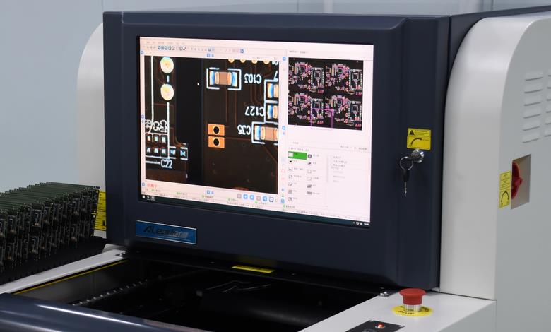
Inspection and Testing: After soldering, the assembled PCB undergoes visual inspection and testing to detect any defects such as soldering defects, component misalignment, or electrical issues. Automated optical inspection (AOI) and in-circuit testing (ICT) are commonly used for this purpose.
Cleaning (if applicable): If required, the PCB assembly may undergo a cleaning process to remove any residual flux or contaminants left from the soldering process. This ensures the long-term reliability of the PCB assembly.
Final Assembly and Packaging: Once the PCB assembly passes inspection and testing, any remaining assembly steps such as attaching connectors, mounting components, and final testing may be performed. The assembled PCBs are then packaged according to the specific requirements of the product.
These steps may vary slightly depending on factors such as the complexity of the PCB design, the type of components used, and the manufacturing processes employed by the assembly facility.
10. What does a PCB assembler do?
A PCB (Printed Circuit Board) assembler is responsible for assembling electronic components onto printed circuit boards according to design specifications. Their duties typically include:
Component Placement: Following assembly instructions and diagrams, the assembler places electronic components, such as resistors, capacitors, integrated circuits, and connectors, onto the PCB.
Soldering: Using soldering irons or automated soldering equipment, the assembler solders the components onto the PCB to establish electrical connections.
Quality Control: Inspecting the assembled PCBs for defects, ensuring proper alignment of components, correct soldering, and adherence to quality standards.
Testing: Conducting functional tests or collaborating with quality assurance teams to ensure that the assembled PCBs meet performance requirements and specifications.
Troubleshooting: Identifying and rectifying any issues or defects found during testing or inspection, which may involve rework or repair of components.
Documentation: Maintaining accurate records of assembly processes, component specifications, and any issues encountered during assembly for quality assurance and traceability purposes.
Equipment Maintenance: Performing routine maintenance and calibration of assembly equipment to ensure proper functioning and accuracy.
Overall, PCB assemblers play a crucial role in the manufacturing process of electronic devices by accurately assembling and testing PCBs to ensure their functionality and reliability.


